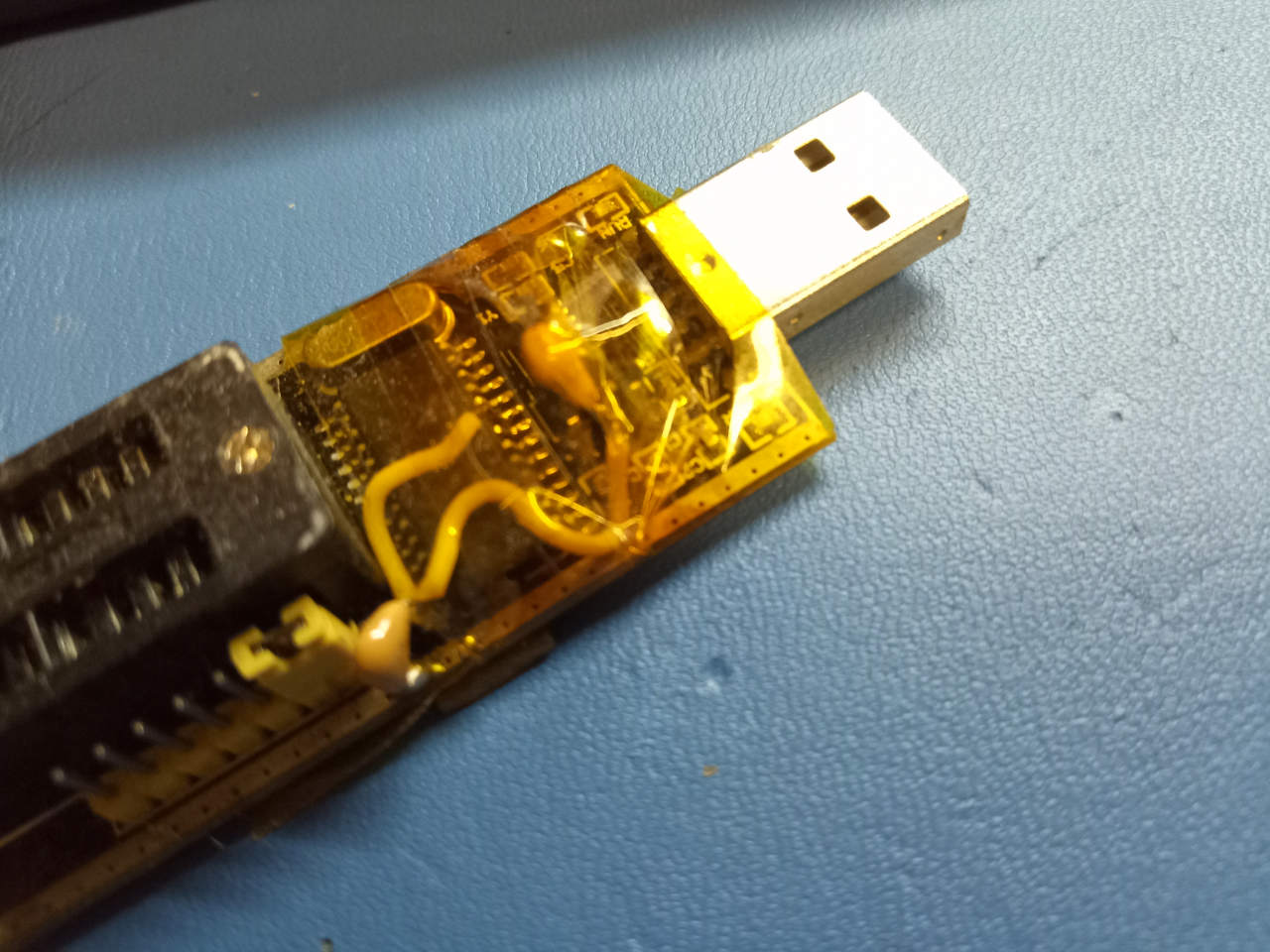
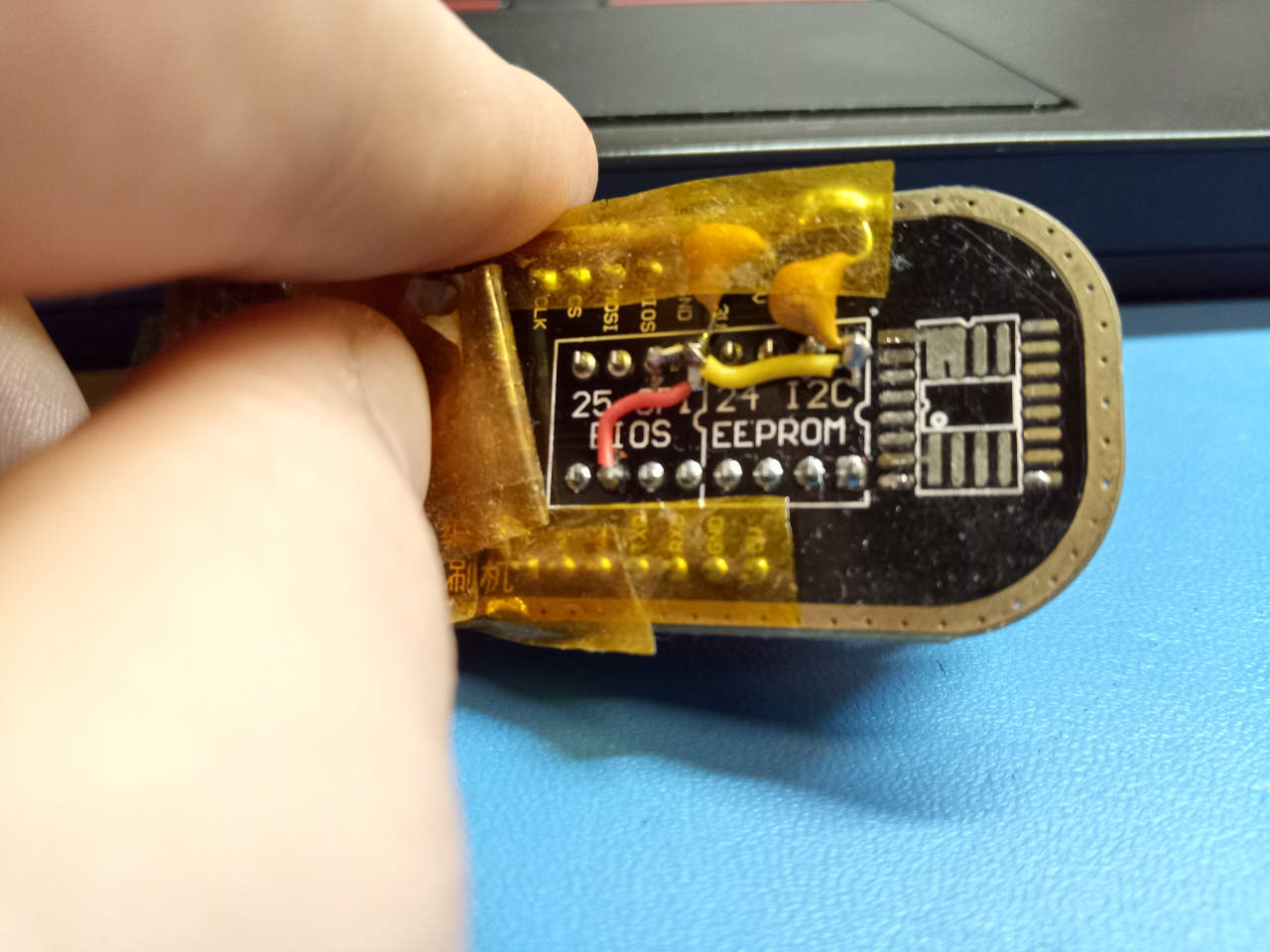
Read/write 25XX NOR flash via SPI protocol
- Home
- FAQ
- Download
- Git
- Buy Libreboot preinstalled / coreboot send-in service
- Install
- Docs
- News
- RSS
- Bugs
- Contact
- Donate
If you want professional Libreboot installation, an installation service is available; it also offers other coreboot firmware besides Libreboot. For example, Chromebook installation via MrChromebox UEFI coreboot distribution is also available.
VOLTAGE WARNING
WARNING: Do NOT assume that the voltage is 3.3v on what you’re flashing. Lots of modern flash chips today are 1.8v on a lot of newer systems. Please always check the letting on the chip and then look up a datasheet, to tell exactly what voltage it’s rated for; measuring with a volt meter would also be prudent.
CAN’T GET A VALID READ??
On systems that have two flash chips, MISO/MOSI are shared on a common line hooked up to the PCH, but each flash has its own chip select. The PCH will turn each chip on and off as required, when reading to or writing to a certain chip. When externally flashing, both chip selects may be floating, so both chips may be active.
In practice, many boards may place a small amount of resistance between MISO/MOSI between the two flashes, such that the floating clip select isn’t really all that bad. When you hook up your flasher, you will typically control the chipselect on the one you’re flashing, but again the chip select on the other flash may be floating.
Chip select is active low, so pulling it high turns off the chip. Assuming you don’t have other issues, e.g. bad wires, or wires too long, or unreliable flasher, you should rule that out and pull the other chipselect high. E.g. if you’re flashing SPI1, make sure SPI2’s chipselect is held high (shorted to 3.3v).
Other than that, you should also check that your flasher has good drive level, e.g. CH341a is pretty weak for in-system programming and should not be used in most cases.
It they both fit, you could just use a 2nd clip on the other chip you want to turn off, and control the chip select using that.
Trouble?
Inquiries can be made via Libreboot IRC and other channels.
If you want professional installation, Minifree Ltd sells Libreboot pre-installed on select hardware, and it also provides a Libreboot preinstall service if you want to send your machine in to have Libreboot installed for you.
Leah Rowe, the founder and lead developer of Libreboot, also owns and operates Minifree Ltd; sales provide funding for the Libreboot project.
Install open source BIOS/UEFI firmware
This guide is predominantly about installing Libreboot (flashing it) onto your motherboard’s main system flash. You can also adapt this guide for dumping, erasing and verifying firmware images; this guide shows you how to use the flashprog software with various external 25XX NOR flash programmers. This guide is written for Linux users, but BSD operating systems are also compatible with flashprog; Windows might be feasible, ditto Apple’s MacOS, as flashprog can also run on those, but they are not officially supported by Libreboot, and we recommend that you use Linux/BSD.
Although this documentation is written for the Libreboot project, it can be used on any compatible 25xx NOR flash, on any number of devices, such as home routers and even certain videogame systems. If you’re a refurbisher, and not a Libreboot-based one, but just a regular refurbisher e.g. on eBay, dealing with proprietary UEFI firmware (and perhaps Windows installations), it may be that on some of them, SMM-based flash writes are performed to store UEFI firmware configurations (instead of the old NVRAM/CMOS memory); you could adapt this guide (and read flashprog documentation) to erase/flash custom configurations, for example when unlocking boot passwords on the computers that you sell. This is the power of Free Software; flashprog is a Free Software project. The use-case scenario of the humble eBay seller is real; several of them have in fact used this guide in the past.
So keep that in mind; this is part of the Libreboot installation instructions, but it can be used for any flashing operation on any 25xx NOR flash, with all sorts of firmware; you could also use this to reverse a Libreboot installation, re-flashing the original vendor firmware if you made a dump of it, and we definitely recommend backing that up prior to Libreboot installation.
Please ensure that your programmer’s voltage matches that of the flash IC, and read this guide carefully to account for proper electrical safety. In general, these programmers operate at 3.3v, so you’ll need a logic level adapter and e.g. buck converter, if you’re dealing with a 1.8V flash IC.
NOTE: Libreboot standardises on flashprog now, as of 27 January 2024, which is a fork of flashrom. The reason why was explained, in the Libreboot 20240225 release
PLEASE READ THESE INSTRUCTIONS BEFORE INSTALLING, OR YOU MAY BRICK YOUR MACHINE!! - Please click the link and follow the instructions there, before flashing. For posterity, here is the link again.
This guide will teach you how to use various tools for externally reprogramming a 25xx NOR flash via SPI protocol. This is the most common type of flash IC for computers that coreboot runs on. Almost every system currently supported by libreboot uses this type of boot flash; the only exception is ASUS KFSN4-DRE, which uses LPC flash in a PLCC32 socket, which you can simply hot-swap after booting the vendor firmware, and then flash internally. Simple!
We will be using the flashprog software which is written to dump, erase and rewrite these flash chips.
Libreboot currently documents how to use these SPI programmers:
- Raspberry Pi Pico / Pico 2
- Raspberry Pi (RPi) single-board computers
- BeagleBone Black (BBB)
- Libre Computer ‘Le Potato’
Many other SPI programmers exist. More of them will be documented on this page, at a date in the future. You can otherwise figure it out on your own; certain parts of this page are still useful, even if you’re using a programmer that Libreboot does not yet document.
Most systems in libreboot have to be re-flashed externally, using instructions on this and similar guides, the first time you flash. However, on all currently supported systems, it’s possible that you can re-flash internally when libreboot is running.
Internal flashing means that the host CPU on your system can re-program the SPI flash, using an on-board SPI programmer (which all boards have). You do this from Linux, with flashprog.
This guide that you’re reading now is for using an external programmer. It is called external because it’s not the internal one on your motherboard.
Raspberry Pi Pico
Pico 1 (RP2040) supported
Pico 2 (RP2530) support was removed, due to stability issues. Pico 1 dongles work just fine (RP2040). Pinout:
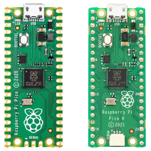
If you don’t already have a programmer, get this one! It’s well engineered, safe, and costs just $5 with headers pre-soldered (Raspberry Pi Pico H). Additionally, all the software running on it is free, down to the full Boot ROM. The wireless versions (Pico W & Pico WH) need vendor firmware to use the Wi-Fi chip, but that is not needed for following this guide.
Download serprog firmware pre-compiled
Download the pico serprog tarball from Libreboot releases. For example, the Libreboot 20241206rev8 one would be named: libreboot-20241206rev8_pico_serprog.tar.xz - it’s available under the roms/ directory in each release. With these binaries, you can easily get started.
Build serprog firmware from source (OPTIONAL)
Pre-compiled binaries are also available, in Libreboot releases.
You can alternatively download the serprog firmware here:
https://codeberg.org/libreboot/pico-serprog
or here:
https://notabug.org/libreboot/pico-serprog
You can also find the source code for these, under src/ in Libreboot release archives (source code tarball), and/or under src/ in lbmk.git if downloading using the build instructions below.
Alternatively to the binaries, you could build it yourself or you could also clone lbmk.git and install build dependencies, then inside lbmk, do:
./mk -b pico-serprogThis will automatically build the rpi-pico firmware, and the file will be at bin/serprog_pico/serprog_pico.uf2 and bin/serprog_pico/serprog_pico_w.uf2.
Install the serprog firmware
First, connect just the Pico to your computer with a micro-USB cable. Mount it like any other USB flash drive. If it isn’t detected, you might need to press the BOOTSEL button while you plug it in (this forces it into the bootloader mode).
When you have the build, or if you’re using a release build, copy the file .uf2 file into your Pico. You must make sure to build the correct target, or otherwise copy the correct file for your device.
Logic levels
A Pico has proper 3.3V logic levels, unlike a ch341a. Which means it won’t destroy your board by sending 5V to it. If you have a 1.8V flash chip, you need to add a logic level converter. Please ensure that you have matched the voltage of your programmer to the voltage of your chip; both the data lines and power lines to the chip must match.
Wiring
Disconnect the Pico and proceed to wire it to your flash chip.
NOTE: SCK and CLK mean the same thing. The diagram below says SCK, and other parts of this guide say CLK. It’s the same thing!
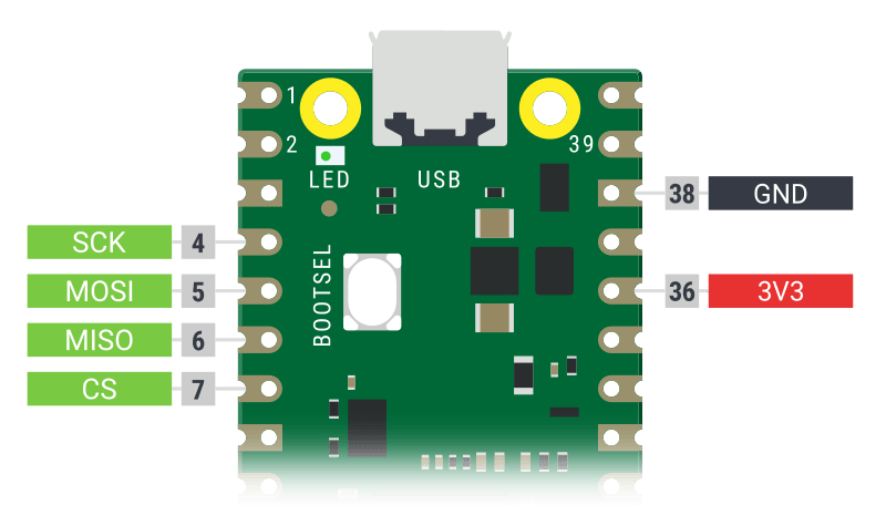
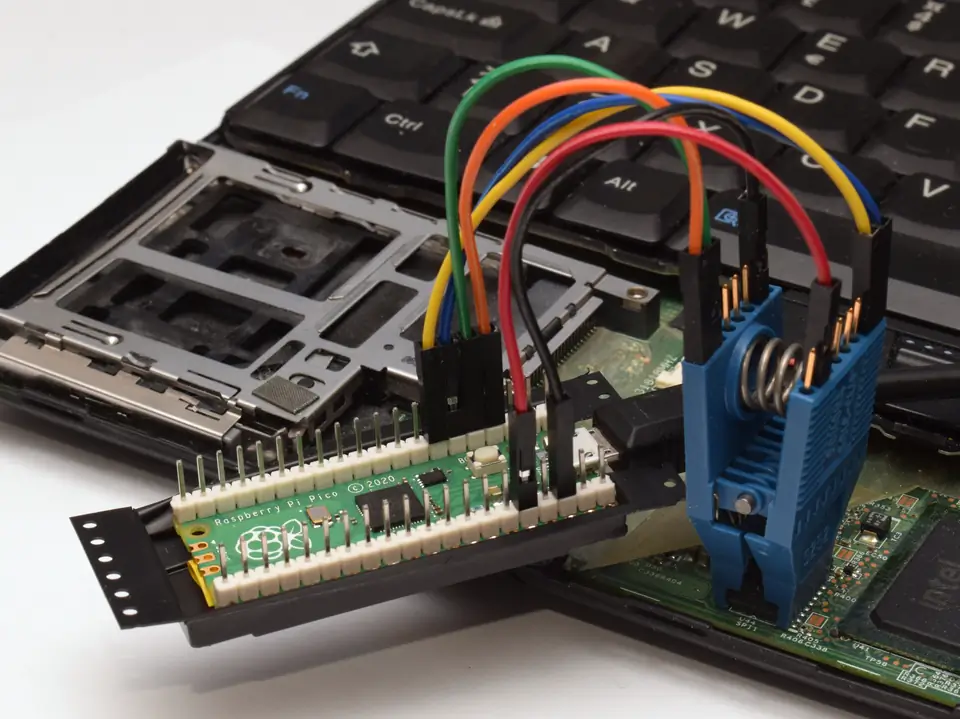
Headers were manually soldered on the top side, and the plastic packaging was repurposed as an insulating base. These might be nice to have, but by no means necessary. If your headers are on the other side, just keep in mind that the pinouts are as seen from above.
Now run (as root) dmesg -wH. When you plug in the Pico, a line like this will appear:
[453876.669019] cdc_acm 2-1.2:1.0: ttyACMx: USB ACM deviceTake note of the ttyACMx. Flashprog is now usable (substitute ttyACMx with what you observed earlier).
flashprog -p serprog:dev=/dev/ttyACMx,spispeed=16Mspispeed=32M usually works, but since it’s not much faster it’s probably not worth it. The 12Mbps USB port is limiting the actual speed here.
Higher speeds might work nicely, on Pico 2.
Do not buy CH341A!
NOR flashes on libreboot systems run on 3.3V DC or 1.8V DC, and this includes data lines. CH341A can have 5V logic levels on data lines, which can damage your SPI flash and also the southbridge that it’s connected to, plus anything else that it’s connected to.
These ch341a programmers are unfortunately very popular. DO NOT use it unless you have fixed the issue. You CAN fix it so that the data lines are 3.3v, if you follow the notes here:
https://www.eevblog.com/forum/repair/ch341a-serial-memory-programmer-power-supply-fix/
In practice, most people will not fix their ch341a and instead just risk it, so no documentation will be provided for ch341a on this website. It is best to discourage use of that device.
Not covered on that eevblog page: the WP/HOLD pins (pins 3 and 7) must be held high via pull-up resistors, but on CH341A dongles, they are directly connected to 3.3V DC (continuity with pin 8). It is advisable to cut these two connections, to the WP and HOLD pins, and jump the cuts using pull-up resistors instead. A value between 1k to 10k (ohms) should be fine.
In the event of a surge, like for example you connect the clip wrongly and cause a short circuit between two pins, lack of pull-up resistors on WP/HOLD could cause a direct short between VCC/ground, which would cause a lot of heat build up and possibly fire (and definitely damaged circuitry). On SOIC8, pin 3 is WP and 4 is GND, so a direct 3.3v connection there is quite hazardous for that reason; all the more reason to use a pull-up resistor.
The motherboard that you want to flash (if using e.g. pomona clip) will probably have pull-up resistors on it already for WP/HOLD, so simply cutting WP/HOLD on the CH341A would also be acceptable. The pull-up resistors that you place (in such a mod) on the CH341A are only useful if you also want to flash chips in the ZIF socket. If pull-up resistors exist both on e.g. the laptop motherboard and on the CH341A, it just means the equivalent series resistance will be of the two resistors (on each line) in parallel. If we assume that a laptop is likely to have a resistor size of ~3.3k for pull-ups, then a value of ~5.6k ohms on the CH341A side seems reasonable.
Alternatively, you might work around the voltage issue by using an adapter with logic-level converter, making sure to have matching vcc going into the flash. Use of a logic level converter would be quite flexible, in this scenario, and you could use it to set many voltages such as 1.8v or 3.3v.
In case it’s not clear:
Please do not buy the ch341a! It is incorrectly engineered for the purpose of ROM flashing on systems with 3.3v SPI (which is most coreboot systems). DO NOT USE IT! This issue still isn’t fixed by the manufacturer, and it doesn’t look like they will ever fix it.
If you see someone talking about CH341A, please direct them to this page and tell them why the CH341A is bad.
These photos show both modifications (3.3v logic and WP/HOLD pull-up resistors) performed, on the black CH341A:


The green version (not shown above) may come with 3.3v logic already wired, but still needs to have pull-up resistors placed for WP/HOLD. Some of them may have switchable voltage instead, via a physical toggle on the board.
Disclaimer: A few (not many, but wily) people have criticised this section of the documentation, due to a misconception about what it really means and also because this section was previously very poorly written. So to be clear:
Yes, we are quite well aware that the CH341A can in fact operate at 3.3v, even unmodified black models; the VCC line is 3.3v, and if when you either directly wire VCC to WP/HOLD pins yourself, or a pull-up resistor on the motherboard you’re flashing pulls these high at 3.3v, then the logic levels on the data lines do in fact switch to 3V during an erase, read or write cycle. When no flashing operation is underway, the data lines are outputting at almost negligable current, so the actual amount of heat generated will be negligable, and therefore damage is unlikely. However, as stated above and as we will state again:
- This is bad electrical design. The CH341A can switch flexibly between 3V and 5V operation, but most flashes today are 1.8V or 3V anyway, and there are all kinds of scenarios (such as over-current or surge event) where this 5V idle logic level could still be applied. Modifying your CH341a to 3.3v only, as defined in the datasheet (and by this page) is highly recommended.
- The drive level is extremely poor anyway, on CH341a, making ISP-based flashing ill advisable in many cases, such as where the PCH (Intel platforms) is partly active and the data lines have lower resistance, because some boards have 0ohms or very low resistance on these lines.
- No pull-ups on the WP/hold lines, when flashing in the socket; they are high via 0ohm trace to VCC, whereas you are advised to use a pull-up resistor to mitigate over-current events.
- Crap LDO on the board, and no ESD/overcurrent protection; the CH341a probably can’t provide much current on the VCC line, especially for ISP-based flashing where the flash shares a common power rail with many other components.
CH341a is cheap junk. Get yourself a Raspberry Pi Pico instead; it’s about the same price, but of much higher quality from an electrical design perspective, supports much higher (12mA!) drive levels on data lines, can control multiple chip selects at once; it’s just better, in every way. And the Raspberry Pi is completely reprogrammable, so you can use it for something else when you’re done, e.g. UART dongle, or if you’re wily enough, PlayStation 1 Optical Disc Emulator - the Pico is simply a highly versatile tool, much better value for money.
There is only one instance where the CH341a is good, and that is when you’re actually flashing a loose (not soldered) chip, in the ZIF socket on the CH341a board. It’s a DIP-8 socket, and you can also buy WSON-8 and SOIC-8 or SOIC-16 adapters for it; you can also plug a special adapter board into it that converts the voltages (VCC and data lines) to 1.8V, for 1.8V flashes (you could also use that same 1.8V adapter circuit in a breadboard wired to your Pico). On socket-based flashing, which is specifically what the CH341a was designed for, you don’t have to worry about weak drive level because there is nothing contending with it on the flash IC’s data pins.
The socket-based flashing operation is what we recommend this programmer for, only if you already have one. We still recommend fixing the issue with the WP/HOLD pins as described above; if you’re doing this, note that there are also newer models that have a voltage switch and logic level shifter already on the board, which can be very useful. Clip-based flashing (ISP / in-system programming) is, specifically, what we advise against using the CH341a for.
Why pay $10 for a CH341a when you can pay $10 for a Raspberry Pi Pico which is electrically and functionally superior in every way? And the Pico is completely open source, right down to the boot rom.
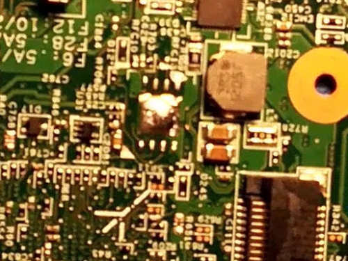
Identify which flash type you have
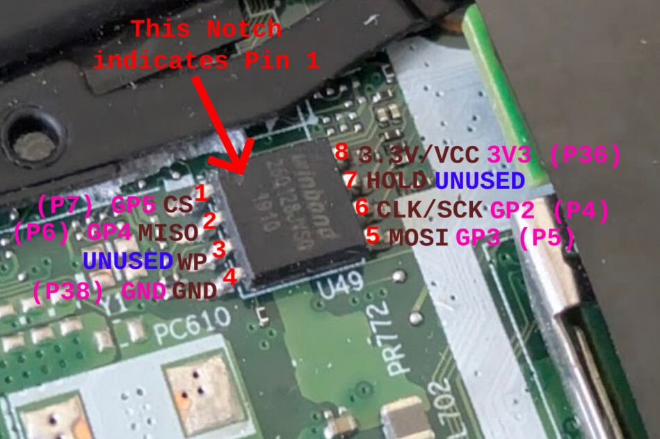
In all of them, a dot or marking shows pin 1 (in the case of WSON8, pad 1).
Use the following photos and then look at your board. When you’ve figured out what type of chip you have, use that knowledge and the rest of this guide, to accomplish your goal, which is to read from and/or write to the boot flash.
SOIC8
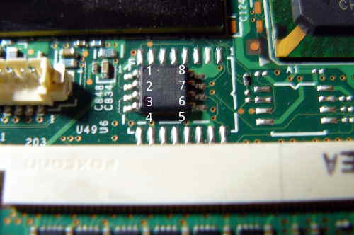
| Pin | Function |
|---|---|
| 1 | CS |
| 2 | MISO |
| 3 | WP |
| 4 | GND |
| 5 | MOSI |
| 6 | CLK |
| 7 | HOLD |
| 8 | VCC |
SOIC16
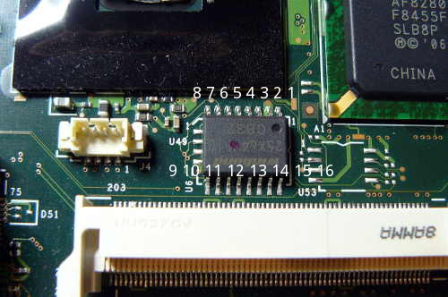
| Pin | Function |
|---|---|
| 1 | HOLD |
| 2 | VCC |
| 7 | CS |
| 8 | MISO |
| 9 | WP |
| 10 | GND |
| 15 | MOSI |
| 16 | CLK |
SOIC8 and SOIC16 are the most common types, but there are others:
WSON8
It will be like this on an X200S or X200 Tablet:
 Pinout is the same as SOIC8 above.
On T400S, it is in this location near the RAM:
NOTE: in this photo, the chip has been replaced with SOIC8.
DIP8
Pinout is the same as SOIC8 above.
Supply Voltage
Historically, all boards that Libreboot supports happened to have SPI NOR chips which work at 3.3V DC. With the recent addition of Chromebooks whose chips are rated for 1.8V DC, this can no longer be assumed.
Inspect the chip on your board for a part number, look up the datasheet for it. Find out and make note of the power supply voltage it needs. If it doesn’t match the voltage output by your external flashing hardware, you should only connect it to the chip through an adapter or logic level converter, never directly.
Software configuration
General/Le potato
The generic guide is intended to help those looking to use an SBC which is not listed in this guide. The guide will, however, use the libre computer ‘Le Potato’ as a reference board. If you have that board, you should refer to the generic guide.
BeagleBone Black (BBB)
SSH into your BeagleBone Black. It is assumed that you are running Debian 9 on your BBB. You will run flashprog from your BBB.
NOTE: This section is out of date, because it is written for Debian 9 (running on the BBB)
Run the following commands as root to enable spidev:
config-pin P9.17 spi_cs
config-pin P9.18 spi
config-pin P9.21 spi
config-pin P9.22 spi_sclk
Verify that the spidev devices now exist:
ls /dev/spidev*Output:
/dev/spidev1.0 /dev/spidev1.1 /dev/spidev2.0 /dev/spidev2.1Now the BBB is ready to be used for flashing. The following systemd service file can optionally be enabled to make this persistent across reboots.
[Unit]
Description=Enable SPI function on pins

[Service]
Type=oneshot
ExecStart=config-pin P9.17 spi_cs
ExecStart=config-pin P9.18 spi
ExecStart=config-pin P9.21 spi
ExecStart=config-pin P9.22 spi_sclk
RemainAfterExit=yes

[Install]
WantedBy=multi-user.target
Now test flashprog:
./flashprog -p linux_spi:dev=/dev/spidev1.0,spispeed=512It is important to use spispeed=512 or a lower number such as 256 or 128, because otherwise the BBB will be quite unstable.
Example output:
Calibrating delay loop... OK.
No EEPROM/flash device found.
Note: flashprog can never write if the flash chip isn't found automatically.
This means that it’s working (the clip isn’t connected to any flash chip, so the error is fine).
Caution about BBB
BeagleBone Black is not recommended, because it’s very slow and unstable for SPI flashing, and nowadays much better options exist. We used to mainly recommend the BBB, because of the fact that it can be used with entirely Free Software on it, but nowadays there are superior options.
TODO: document other SPI flashers
Rasberry Pi (RPi)
SSH into your Raspberry Pi. You will run flashprog from your Raspberry Pi.
You must configure spidev on your Raspberry Pi. This is a special driver in the Linux kernel; technically, the driver name is spi-bcm2835.
This page has info:
https://www.raspberrypi.com/documentation/computers/raspberry-pi.html#spi-overview
In your Raspberry Pi, which we assume you’re running the latest Raspbian version on, do this:
sudo raspi-configUnder the Interface section, you can enable SPI.
The device for communicating via SPI as at /dev/spidev0.0
RPi Drive Strength
Flashprog on the RPi may not be able to detect the SPI flash chip on some systems, even if your wiring and clip are set up perfectly. This may be due to the drive strength of the Raspberry Pi GPIOs, which is 8mA by default. Drive strength is essentially the maximum current the pin can output while also maintaining the minimum high-level voltage. In the case of the Pi, this voltage is 3.0V.
Similarly, the SPI flash chip has a minimum voltage it will accept as a high logic value. This is commonly 0.7*VCC for SPI flash, which is 2.31V for 3.3V chips. If the drive strength is too low, the voltage at the pins of the flash chip may fall below this minimum voltage, causing it to register as a low logic value instead of the high value that was sent.
On many systems, the VCC pin of the SPI flash is shared with other chips on the system, causing them to be powered through the voltage supplied through your programming clip. In this case, parts of the chipset may power up, and it may attempt to set the SPI lines high or low, interfering with the data the Pi is trying to send. If the Pi and chipset are trying to set a pin to different values, the side with a greater drive strength will be able to “pull” the voltage toward the level it wants to set.
Fortunately, the drive strength of the Raspberry Pi can be increased up to 16mA. There are a few tools that can set this, such as the pigs utility from the pigpio project. On the Raspberry Pi OS, the following commands should install pigpio and set the drive strength to 16mA:
Install pigpio:
sudo apt install pigpioStart the pigpiod daemon, which the pigs utility communicates with to interact with the gpios:
sudo pigpiodSet the drive strength of GPIO group 0, which contains the spi0 pins, to 16mA:
pigs pads 0 16 Note that the drive strength hardware works in multiples of 2mA, and pigs will round odd values up to the next multiple of 2. You can check the current drive strength using
pigs padg 0WARNING: If the chipset is very strongly trying to drive a pin to a value opposite that of the Pi, more than 16mA pass through the Pi’s GPIO pins, which may damage them as they are only designed for 16mA. The drive strength is NOT a current limit. That said, this is a risk to the Pi regardless of the drive strength. Resistors between the chipset and the flash should protect against this, though not all boards have these.
See https://www.raspberrypi.com/documentation/computers/raspberry-pi.html#gpio-pads-control for more information about the drive strength control on the Pi.
Caution about RPi
Basically, the Raspbian project, now called Raspberry Pi OS, put in their repo an update that added a new “trusted” repository, which just so happened to be a Microsoft software repository. They seem to have done this for VS Code, but the problem here is that it gave Microsoft free reign to define whatever dependencies they liked (as per apt-get rules), and every time you updated, you would be pinging Microsoft servers. Do you think that is strange?
Microsoft shouldn’t have any access to your Linux system! This was the commit that Raspbian added to their distro, which added this what should rightly be called a security vulnerability, intentionally:
They then removed it, after a public backlash, via the following commits:
- https://github.com/RPi-Distro/raspberrypi-sys-mods/commit/ed96790e6de281bc393b575c38aa8071ce39b555
- https://github.com/RPi-Distro/raspberrypi-sys-mods/commit/4d1afece91008f3787495b520ac03b53fef754c6
Libre firmware on RPi
The boot firmware on older Raspberry Pi models can be replaced, with entirely libre firmware. This may be a useful additional step, for some users. See:
Website:
Install flashprog
If you’re using a BBB or RPi, you will do this while SSH’d into those.
Flashprog is the software that you will use, for dumping, erasing and rewriting the contents of your NOR flash.
In the libreboot build system, from the Git repository, you can download and install flashprog. Do this after downloading the lbmk Git repository:
cd lbmk
sudo ./mk dependencies ubuntu2004
NOTE: debian, arch or void can be written instead of ubuntu2004. the debian script is also applicable to newer ubuntu versions
./mk -b flashprogIf the ubuntu2004 script complains about missing dependencies, just modify the dependencies config to remove those dependencies. The script is located at config/dependencies/ubuntu2004 and it is written for Ubuntu 20.04, but it should work fine in other Linux distributions that use the apt-get package manager.
A flashprog/ directory will be present, with a flashprog executable inside of it. If you got an error about missing package when running the dependencies command above, tweak config/dependencies/ubuntu2004. That script downloads and installs build dependencies in apt-get and it is intended for use on x86-64 systems running Ubuntu 20.04, but it should work in Raspbian on the Raspberry Pi.
Alternatively, you may download flashprog directly from upstream at https://flashprog.org/Flashprog
If you’re flashing a Macronix flashchip on a ThinkPad X200, you will want to use a special patched version of flashprog, which you can download here: https://vimuser.org/hackrom.tar.xz - patched source code is available, and a binary is also available that you can simply run. Pass the --workaround-mx argument in flashprog. This mitigates stability issues.
If you downloaded the flashprog source code directly, you can go into the directory and simply type make. In the libreboot build system, build dependencies are documented in configuration files located at config/dependencies/ which you can install using the apt-get software.
How to use flashprog
Read past these sections, further down this page, to learn about specific chip types and how to wire them.
Reading
Before flashing a new ROM image, it is highly advisable that you dump the current chip contents to a file.
Run this command to see if 25xx flash is detected, with your RPi properly wired.
sudo ./flashprog -p linux_spi:dev=/dev/spidev0.0,spispeed=32768For BBB, you must use a lower speed and a different device path:
sudo ./flashprog -p linux_spi:dev=/dev/spidev1.0,spispeed=512On BBB, never use a speed higher than spispeed=512. In some cases, you may even need to go as low as spispeed=128. The BBB is highly unstable and unreliable for SPI flashing. When you’re reading, take multiple dumps and verify that the checksums match, before you flash. You may have to flash your chip several times!
NOTE: On some systems, higher speeds will be unstable. On those systems, try lower speed like spispeed=4096 or even spispeed=2048 which should, in most cases, work just fine but it will obviously be slower. The spispeed=32768 setting works just fine on most setups if you use short wires, within 10cm.
If flash chip is detected you may try reading (dumping) the flash contents now, or you can try flashing it with a new ROM.
Dump it like so (RPi):
sudo ./flashprog -p linux_spi:dev=/dev/spidev0.0,spispeed=32768 -r dump.binFor BBB, do this:
sudo ./flashprog -p linux_spi:dev=/dev/spidev1.0,spispeed=512 -r dump.binIt is advisable to take a 2nd dump, e.g. dump2.bin, and then check sha1sum:
sha1sum dump*.binIf the checksums match, it indicates that you have a good dump. If they do not, check your wiring. Wires should be within 10cm length for best stability, and they should all be the same length (VCC and GND wires can be longer).
This advice is especially applicable to the BBB, which is highly unreliable.
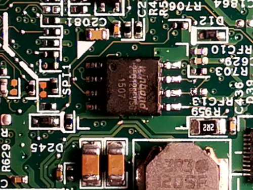
For boards with more than one flash chip you will need to read from both chips and combine them into a single file. Most of the time, a two chip setup includes one 8mb chip (SPI1) and one 4mb (SPI2) chip. SPI1 is the first 8MB of the ROM image in this example. The setup just described applies to the x230, t430, t530, and t440p. For other boards, make sure you know which chip contains the lower and upper portions of the rom. You can combine both flashes together with cat for example:
cat spi1_8mb.rom spi2_4mb.rom > full_12mb.romNote that you will need this combined rom if you intend to manually extract vendor files, which is a method not officially supported by Libreboot’s build system.
Writing
Next, run this command (RPi):
sudo ./flashprog -p linux_spi:dev=/dev/spidev0.0,spispeed=32768 -w /path/to/libreboot.romIf using BBB:
sudo ./flashprog -p linux_spi:dev=/dev/spidev1.0,spispeed=512 -w /path/to/libreboot.romIf using BBB, you may have to use a lower speed than 512. You may also have to re-flash several times before it works fully.
Again, use a lower spispeed value if you need to, for stability.
Once that command outputs the following, the flash has completed successfully. If not, just flash again.
Reading old flash chip contents... done.
Erasing and writing flash chip... Erase/write done.
Verifying flash... VERIFIED.
If it says “VERIFIED” or says that the chip contents are identical to the requested image, then the chip is properly flashed.
If the board you are writing to has two chips you’ll need to split the rom into two sections. For example, to split a rom for the x230, t430, t530, or t440p run:
dd if=libreboot_12mb.rom bs=1M of=spi1_8mb.rom count=8
dd if=libreboot_12mb.rom bs=1M of=spi2_4mb.rom skip=8
Flash the resulting roms to each of their respective chips according to the above instructions.
Hardware configuration
Refer to the above guidance about software configuration. The following advice will teach you how to wire each type of flash chip.
WARNINGS
Do not connect the power source until your chip is otherwise properly wired. For instance, do not connect a test clip that has power attached.
Do not disconnect your chip from the flasher until you’ve disconnected or turned off the power source.
BE CAREFUL that you are indeed supplying the appropriate supply voltage to the chip. SPI flashes on most of the currently supported libreboot hardware run on 3.3V DC and logic at that level too. Some of them (at least Chromebooks) can have chips that run on 1.8V DC. You should make sure to check the part number and datasheet of the SPI flash chip for the supply voltage it requires. If your external flashing hardware doesn’t match it, use an adapter or logic level converter to flash.
It is important to CHECK that you are running on the correct voltage, when you do anything with these chips. Lower than the rated supply voltage won’t damage anything, but higher will fry your chip (on most 3.3V chips, the tolerated voltage range is between 2.7V and 3.6V, but 3.3V is the most ideal level).
DO NOT connect more than 1 DC power source to your flash chip either! Mixing voltages like that can easily cause damage to your equipment, and to your chip/motherboard.
MISO/MOSI/CS/CLK lines
You may want to add 47ohm series resistors on these lines, when flashing the chips. Only do it on those lines (NOT the VCC or GND lines). This provides some protection from over-current. On Intel platforms, the SPI flash is usually connected via such resistors, directly to the Southbridge chipset.
ISP programming and VCC diode
ISP means in-system programming. It’s when you flash a chip that is already mounted to the motherboard of your computer that you wish to install libreboot on.
It may be beneficial to modify the motherboard so that the SPI flash is powered (on the VCC pin) through a diode, but please note: a diode will cause a voltage drop. The tolerated range for a chip expecting 3.3V VCC is usually around 2.7V to 3.6V DC, and the drop may cause the voltage to fall outside that. If you do this, please also ensure that the WP and HOLD pins are still held to a high logic state; each via their own resistor (1K to 10K ohms) connected to the same power source going through the diode.
The reason is simple: on most systems, the flash shares a common power rail with many other components on the board, which draw a lot of current. Further, if you accidentally provide too much voltage or cause an overcurrent, you could fry those other components but if there is diode protection, you’ll only fry the boot flash (and it is very easy to replace, if you have good soldering skills).
When you’ve placed the diode, ensure that VCC on the chip is isolated from all other components on that board, which share the same power rail. Further, ensure that the pull-up resistors for WP/HOLD are only connected to the side of the diode that has continuity with the VCC pin (this is important because if they’re not, they won’t be held high while doing ISP flashing, even if they’re still held high when the motherboard is fully powered on).
Furthermore: ensure that the SPI flash is operating at the appropriate supply voltage (2.7V to 3.6V for a 3.3V chip) when fully powered on, after installing the diode.
If it’s a desktop/workstation/server board (not a laptop), you could de-solder the SOIC8/WSON8 if it uses that, and replace with an IC socket (for SOIC8, WSON8 or DIP8, whatever you want), because then you could easily just insert the flash into a breadboard when flashing.
TODO: Make a page on libreboot.org, showing how to do this on all motherboards supported by libreboot.
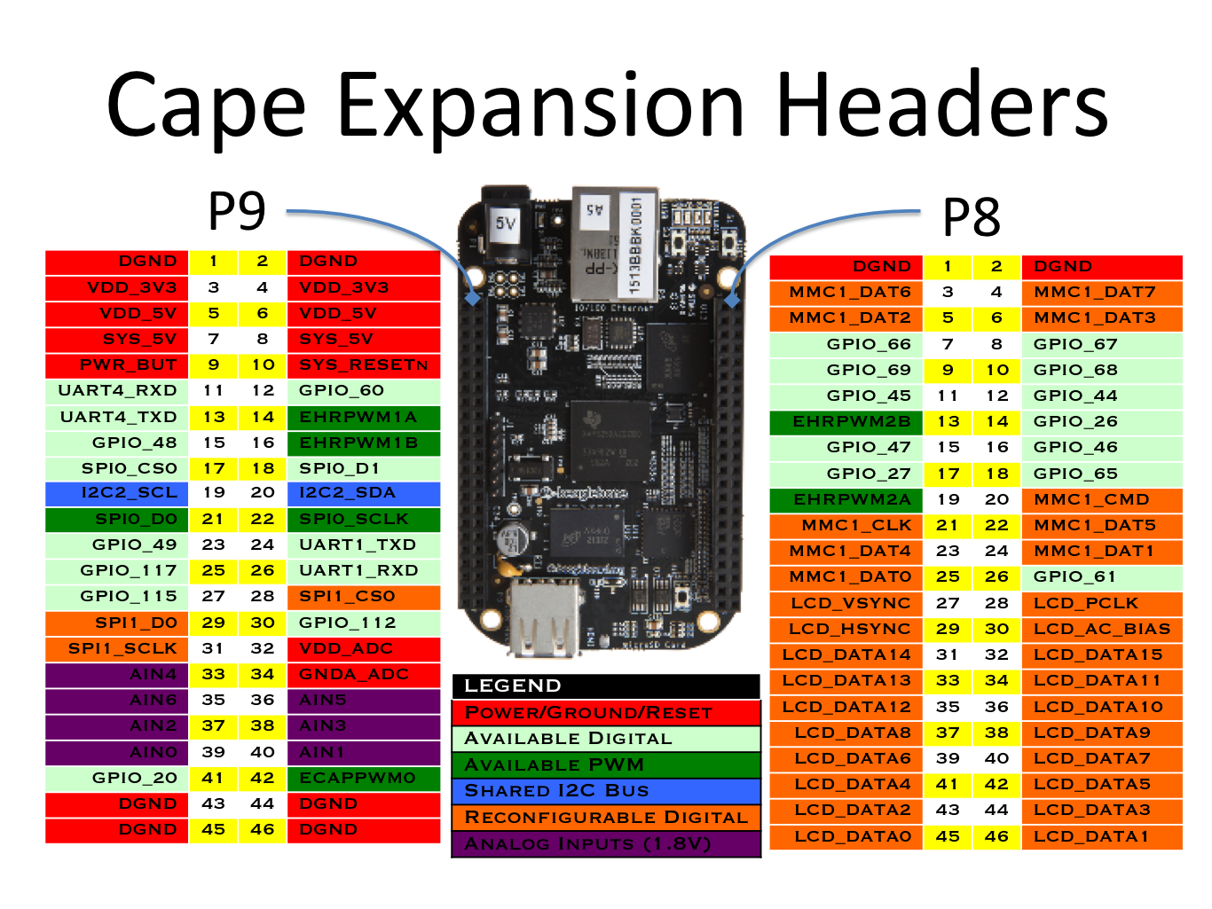
GPIO pins on BeagleBone Black (BBB)
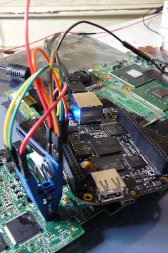
Use this image for reference when connecting the pomona to the BBB: https://beagleboard.org/Support/bone101#headers (D0 = MISO or connects to MISO).
On that page, look at the P9 header. It is what you will use to wire up your chip for flashing.
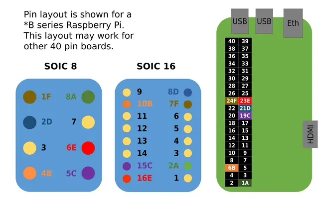
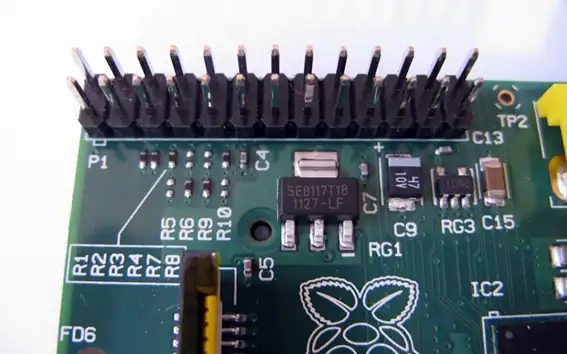
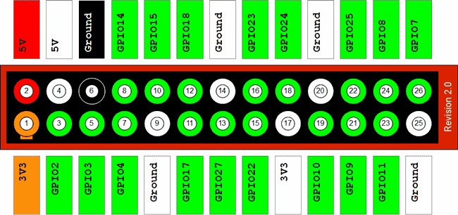
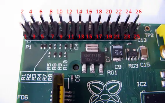
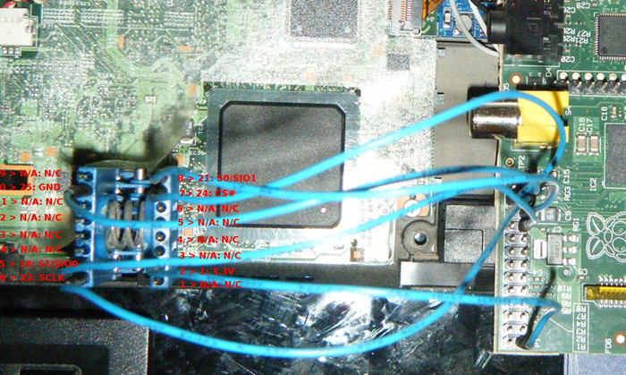
GPIO pins on Raspberry Pi (RPi) 40 Pin
This diagram shows the pinout for most modern Pi’s and Pi derivatives. The diagram shows the pins of an RPi on the left and the two SOIC clips on the left.
GPIO pins on Raspberry Pi (RPi) 26 Pin
Diagram of the 26 GPIO Pins of the Raspberry Pi Model B (for the Model B+ with 40 pins, start counting from the right and leave 14 pins):
Use this as a reference for the other sections in this page, seen below:
SOIC8/DIP8/WSON8 wiring diagram
Refer to this diagram:
| Pin # | 25xx signal | RPi(GPIO) | BBB(P9 header) |
|---|---|---|---|
| 1 | CS | 24 | 17 |
| 2 | MISO | 21 | 21 |
| 3 | not used | not used | not used |
| 4 | GND | 25 | 1 |
| 5 | MOSI | 19 | 18 |
| 6 | CLK | 23 | 22 |
| 7 | not used | not used | not used |
| 8 | VCC | 1 | 3 |
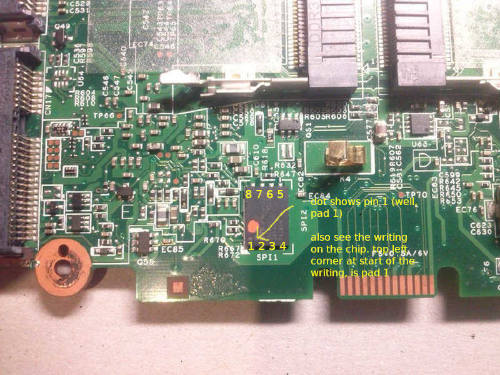
On your SOIC8, there will be a dot in one of the corners. The dot is pin 1.
NOTE: pins 3 and 7 are WP/HOLD pins. If flashing a chip on a breadboard, please use pull-up resistors on those (see notes below), and decoupling capacitor on pin 8 (VCC).
NOTE: On X60/T60 thinkpads, don’t connect pin 8. Instead, plug in your the PSU to the charging port on your motherboard, but do not power on the motherboard. This will provide a stable 3.3V voltage, with adequate current levels. On those laptops, this is necessary because the flash shares a common 3.3V DC rail with many other ICs that all draw quite a lot of current.
SOIC16 wiring diagram (Raspberry Pi)
RPi GPIO header:

BBB P9 header:
https://beagleboard.org/static/images/cape-headers.png
Refer to this diagram:
| Pin # | 25xx signal | RPi(GPIO) | BBB(P9 header) |
|---|---|---|---|
| 1 | not used | not used | not used |
| 2 | VCC | 1 | 3 |
| 3 | not used | not used | not used |
| 4 | not used | not used | not used |
| 5 | not used | not used | not used |
| 6 | not used | not used | not used |
| 7 | CS# | 24 | 17 |
| 8 | MISO | 21 | 21 |
| 9 | not used | not used | not used |
| 10 | GND | 25 | 1 |
| 11 | not used | not used | not used |
| 12 | not used | not used | not used |
| 13 | not used | not used | not used |
| 14 | not used | not used | not used |
| 15 | MOSI | 19 | 18 |
| 16 | SCLK | 23 | 22 |
Refer to the RPi GPIO guide above, on this page.
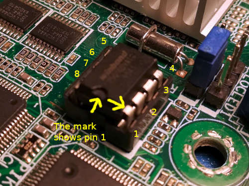
On your SOIC16, there will be a dot in one of the corners. The dot is pin 1.
NOTE: pins 1 and 9 are WP/HOLD pins. If flashing a chip on a breadboard, please use pull-up resistors on those (see notes below), and decoupling capacitor on pin 2 (VCC).
Pull-up resistors and decoupling capacitors
Do this for chips mounted to a breadboard. Ignore this section if you’re flashing a chip that is already soldered to a motherboard.
This section is only relevant if you’re flashing a new chip that is not yet mounted to a motherboard. You need pull-up resistors on the WP and HOLD pins, and decoupling capacitors on the VCC pin. If the chip is already mounted to a board, whether soldered or in a socket, these capacitors and resistors will probably already exist on the board and you can just flash it without pulling WP/HOLD high, and without capacitors(just connect your external power source).
The best way is as follows:
- Insert the DIP8 IC into a breadboard (2.54mm holes), if it’s DIP8
- Insert WSON8 into a WSON8 socket and put on a breadboard, if WSON8
- Insert SOIC8 into a SOIC8 socket and put on a broadboard, if SOIN8
- Wire an SPI flasher, using 2.54mm dupont leads, to the breadboard, using the correct wiring (see link to SPI flashing guides below)
SOIC8/WSON8/DIP8: pin 3 and 7 must be held to a high logic state, which means that each pin has its own pull-up resistor to VCC (from the voltage plane that pin 8 connects to); anything from 1Kohm to 10Kohm will do. When you’re flashing a chip that’s already on a laptop/desktop/server motherboard, pin 3 and 7 are likely already held high, so you don’t need to bother.
SOIC8/WSON8/DIP8: pin 8, which is VCC, will already have decoupling capacitors on it if the chip is on a motherboard, but lone chip flashing means that these capacitors do not exist. A capacitor passes AC but blocks DC. Due to electromagnetic indunctance, and RF noise from high-speed switching ICs, a DC voltage line isn’t actually straight (when viewed on an oscilloscope), but actually has low voltage AC mixed in; on a particularly noisy line under high load, noise of around 300mV or more is common. To smooth out that noise, you wire capacitors from the DC line to ground, with the side of the capacitor on VCC as close to the IC’s VCC pin as possible. We recommend that you use ceramic capacitors for this purpose. The recommended capacitors for this are: 100nF and 4.7uF ceramic capacitors. Electrolytic capacitors are inferior for this, because they have higher ESR (ceramic capacitors have super low ESR, which is very good for decoupling).
The result of using a decoupling capacitor is that some of the noise on the DC line is filtered to ground, making the DC signal much cleaner/straighter (when seen on an oscilloscope).
SOIC16: same as above, but use a SOIC16 socked on a breadboard. On SOIC16, WP/HOLD are not pin 3/7 like above, but instead pins 1 and 9, so wire your pull-up resistors on those. VCC on SOIC16 is pin 2, so wire your decoupling capacitors up on that.
SOIC8/WSON8/DIP8/SOIC16 not mounted to a motherboard
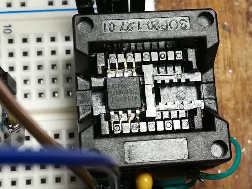
If your system has lower capacity SPI flash, you can upgrade. On most systems, SPI flash is memory mapped and the maximum (in practice) that you can use is a 16MiB chip. For example, KGPE-D16 and KCMA-D8 motherboards in libreboot have 2MiB flash by default, but you can easily upgrade these. Another example is the ThinkPad X200S, X200 Tablet and T400S, all of which have WSON8 where the best course of action is to replace it with a SOIC8 flash chip.
In all such cases, flashing a new chip should be done using a breadboard, not a test clip. You will use 2.54mm dupont leads to connect your Raspberry Pi. For data lines, make sure that all wires are the same length, and about 10cm in length (don’t use longer lengths than this).
Some advice:
- DIP8: Strong choice is Winbond W25Q128FVIQ. It is a direct drop-in replacement
- SOIC8 is possible: Winbond W25Q128FVSIG is a strong choice.
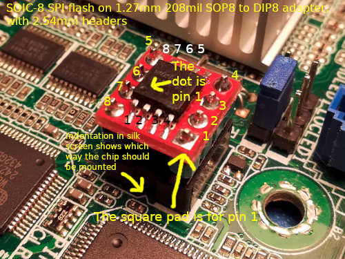
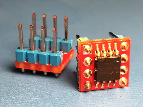
- DIP8 using adapter and SOIC8 is also possible. Use a 208-mil 1.27mm SOP8/SOIC8 to DIP8 adapter PCB with a 2.54mm 4-pin header on each side (square pins), then you can slot that in as though it were a normal P-DIP 8 IC. This page shows a perfect example: https://coolcomponents.co.uk/products/soic-to-dip-adapter-8-pin
- The above SOP8/DIP8 adapter is actually what we recommend, if you’re going that route. It’s made by Sparkfun and widely available; you don’t have to buy from that particular website. The part number is: BOB-13655
- If you use a SOP/DIP adapter with a SOIC8 IC, you’ll have to solder it obviously. K tip is a nice choice for soldering ICs like these. Use good flux and 60/40 leaded solder (or 63/37), none of that Rohs lead-free crap.
If you go for a SOIC8, mounted it to the SOP to DIP adapter (208mil 1.27mm one) and solder 2.54mm headers to it. You could put the 2.54mm pins in a breadboard, then solder the chip to the adapter PCB and mount that to the pins on the breadboard, to keep it aligned, and solder that. Whith the PCB on the pins, and the pins in the breadboard, push the pins inwards a little bit.
This is for a new SOIC8 chip, but you can get sockets similar to the one in the video, but for WSON8. Sometimes they are called DFN8 or QFN8 sockets. Get one that is 1.27mm pitch.
If you’re flashing/dumping a lone WSON8, get a WSON8/QFN8/DFN8 socket (1.27mm pitch) and mount it to a breadboard for flashing. If your motherboard’s landing pads for the flash IC can take a SOIC8, we recommend that you use a SOIC8 instead because a test clip is possible later on when you wish to re-flash it, however you may be dealing with a board where replacing existing WSON8 with SOIC8 is desirable; in that case, you might still want to dump the contents of the original WSON8.
Here is a SOIC8 in a socket, mounted to a breadboard, for flashing:
Here is a photo of a DIP8 IC:
Here is a photo of a SOIC8 in 1.27mm 208mil SOP to DIP adapter:
NOTE: DIP8 and WSON8-in-socket, and SOIC16-in-socket, are basically the same, just adapt accordingly.
If you’re replacing a DIP8 but using SOIC8 on an adapter, solder it to the adapter first, then insert 2.54mm headers (square pins) into a breadboard to keep them aligned. Put the SOIC8 on the PCB, onto the pins, and push the pins inwards a little bit, and solder that. Alternatively to the breadboard, you can just put the 2.54mm pins directly in the DIP8 socket and mount the SOIC8 + adapter onto that, and solder that. Use quality rosin flux (not acid based) and good 60/40 or 63/37 leaded solder (don’t use lead-free):
SOIC8/SOIC16 soldered to a motherboard
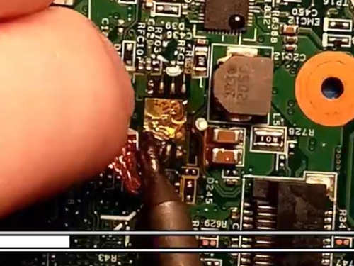
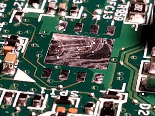
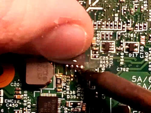
This is an example of in-system programming or ISP for short.
SOIC8:
Pomona 5250 is a SOIC8 test clip. There are others available, but this is the best one. Use that. Use the SOIC8 diagram (see above) to wire up your Raspberry Pi. Your motherboard likely already pulls WP/HOLD (pins 3 and 7) high, so don’t connect these. VCC on SOIC8’s pin 8 probably already has decoupling capacitors on the motherboard, so just hook that up without using a capacitor.
SOIC16:
Pomona 5252 is a SOIC16 test clip. There are others available, but this is the best one. Use that. Use the SOIC16 diagram (see above) to wire up your Raspberry Pi. WP/HOLD pins are pins 1 and 9, and likely already held high, so no pull-up resistors needed. You do not need a decoupling capacitor for pin 2 (VCC) either because the motherboard will already have one.
Here is an example of a test clip connected for SOIC16:
And here is an example photo for SOIC8:
DIP8 soldered to the motherboard
It is extremely cursed for DIP8 to be soldered directly to the motherboard. It is usually mounted to a socket.
The pins are large enough that you can just use test hooks to wire up your chip for flashing. You might want to de-solder the chip, using a solder vacuum (extractor) tool, and then you can install a socket in its place. You can then insert the DIP8 IC into the socket.
In the libreboot project, we have never heard of a board where the DIP8 is directly soldered. It is almost always mounted in a socket.
Your DIP8 IC has the same pinout as a SOIC8 IC.
Replace WSON8 IC with SOIC8
NOTE: You can alternatively purchase WSON8 probes from a site like Aliexpress. They look similar to SOIC8 clips, and they work similarly.
You can connect a SOIC8 test clip, but you will struggle to get good connections and it will be extremely unreliable. DO NOT solder to the pads of the WSON8 directly; some people do this, but you shouldn’t do it, because you can easily damage the pads that way.
WSON8 has the same pinout as SOIC8, but it’s a ball mounted QFN (quad flat pack, no leads). There are no clips for it. Sometimes referred to as QFN8
On all currently supported libreboot hardware, boards that have WSON8 can also have a SOIC8 because the pads are long enough to accomodate either type of chip.
A good choice of soldering iron would be a T12-D08 or T12-K tip, on a T12 soldering station. KSGER makes nice soldering stations:
https://yewtu.be/watch?v=w0nZCK7B-0U
The case on that KSGER station is not grounded by default, so you should modify it to ground the case, in case of an electrical fault. This is for your safety. This video shows how to do it:
https://yewtu.be/watch?v=-6IZ_sBgw8I
Use quality 60/40 or 63/37 lead+tin solder. Do not use lead-free! Lead-free is not suitable for hobbyist use such as this. Use quality rosin flux. Fluxes with an acid base should never be used. Amtech and MG Chemicals make good flux pastes. Use it in a dispenser tube. Some of these fluxes will contain adapic acid which has a low pH level, and it is simply used as a mild activator. So long as you clean the flux afterwards, you should be fine.
Make sure to have a copper wire brush and a wet sponge handy. You wipe the iron on the wire brush and tap it on the wet sponge(to remove oxides) to keep it clean. Always clean your tip constantly. Also, after cleaning it, always re-tin the tip with fresh solder, to prevent the tip from oxidizing!
Make sure to buy 99.9% isopropyl alcohol. Don’t buy weaker solutions because they contain water, and don’t use other chemicals because most other chemicals are corrosive. You use the isopropyl to clean the area you’re soldering, before soldering it, and then soak up the wet alcohol with a cloth. You will also use it to clean off any flux that you used.
Use of flux is very important, to get a good solder joint, because it removes oxides and prevents further oxidation during soldering, ensuring that the solder flows properly, otherwise the solder will ball up and you won’t get a good joint.
In case you’re not comfortable with soldering, we have some excellent videos linked on the FAQ page which you can watch.
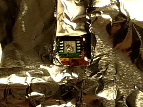
WSON8 IC:
Surround a large area around the chip with layers of kapton tape, and then aluminium foil. This will act as a heat shield, to reduce the risk of re-flowing other solder joints (which can make them turn into cold joints, and you risk knocking them off of the board):

Notice that the kapton+foil does not cover the chip itself, or the solder pads. It’s important that these are exposed to the heat.
Use a hot air rework station, set to about 330-340C. The reason for the higher temperature is because air doesn’t conduct heat as efficiently as an iron, so you must use a higher temperature. You should put lots of rosin flux above the IC. Do not hold the nozel too close to the board. The diameter of the nozel should be slightly higher than the length of the chip. Apply even heat, at high air flow.
While blasting the chip with hot air, hold the chip with tweezers but do not use any real force. Do not try to forcefully pry off the chip. Simply hold the chip with your tweezers, gently nudging it until it feels like the chip can move freely. While in this state, the solder is fully melted and the chip can be lifted off with ease.
If you’re doing it correctly, the chip will come off within 1 minute, like so:
Add fresh solder to the pads, including the thermal pad:
Now wick it out using a copper braid, dunked in rosin flux:
Ensure that all of the solder is removed:
You will notice that one of the pads doesn’t have all of the solder removed. The pad on the top-left in this photo. This is intentional, to show you a comparison for reference. The other pads are free of solder.
You can simply solder the chip unflashed, and flash it using a test clip. Alternatively, you can put the SOIC8 in a socket on a breadboard, and flash it before soldering it. If you wish to dump the contents of the WSON8, you can put the removed WSON8 in a socket on a breadboard and dump it using your SPI flasher.
Align the new SOIC8, and tack it in the corner pins. Then solder it fully. Use lots of flux!
A T12-D08 tip is being used in this photo, but a mini chisel, mini hoof or knife (e.g. T12-K) tip would be ideal.
Ensure that all the joints are perfect. A good solder joint is shiny, and with concave fillets where the solder has flowed. Observe:
After you’re done, use a soft bristle brush and 99.9% isopropyl alcohol to break up the remaining flux, then soak up the flux using a cloth, while the alcohol is still wet. 99.9% isopropyl is the best liquid to use, because it evaporates quickly and it does not leave a corrosive residue.
LICENSING
This page is released under different copyright terms than most other pages on this website.
This page and the photos on it are available under CC BY SA 4.0 Check the Git repository for history of who owns what part of the document.
Photos showing a BeagleBone Black are under the normal GFDL license like other pages and images on this website, or you can use them under the CC-BY-SA 4.0 license if you wish (I, Leah Rowe, own all BBB photos shown on this page, except for the one on the beaglebone website, and that one is merely linked here, instead of being hosted on the av.libreboot.org server).
This version of the page is hosted in the lbwww git repository, with images for it hosted in the lbwww-img repository (from libreboot).
The Canoeboot version of this page is: https://canoeboot.org/docs/install/spi.html
Markdown file for this page: https://libreboot.org/docs/install/spi.md
This HTML page was generated by the Libreboot Static Site Generator.